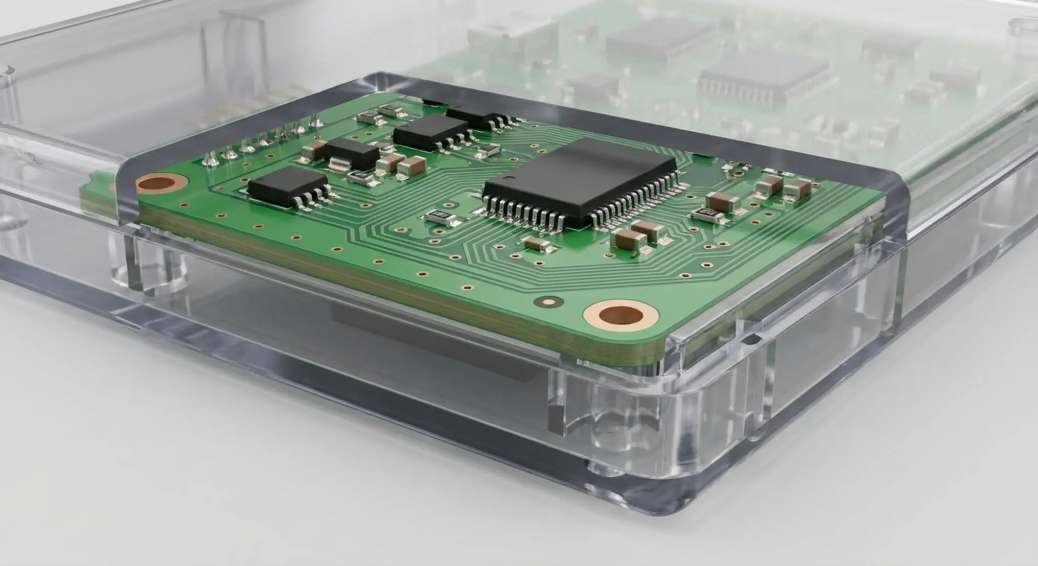
PCB Design: How to Match the Printed Circuit Board to the Product Enclosure
Harmonizing electronics and mechanics from day one to avoid costly redesigns.
In Brief
Matching the printed circuit board to the product enclosure begins with parallel design of electronics and mechanics - not a sequential workflow. The first step requires defining rigid dimensions, fixed positions for external connectors, and exclusion zones where tall components cannot be placed.
Development engineers then use software tools that enable transferring 3D board models into the mechanical design environment. This process makes it possible to detect physical collisions, plan effective heat dissipation mechanisms, ensure stable board anchoring inside the enclosure, and verify that the final product meets all functional and aesthetic requirements.
Over many years of guiding entrepreneurs and leading complex technology projects, we have repeatedly encountered the same frustrating scenario. The electronics team develops a flawless PCB, the mechanical team designs a beautifully crafted enclosure, yet at the moment of truth - when they attempt to combine the two - the components do not fit. Connectors don't seat properly, the cover won't close because of an oversized component, or worse, the device overheats and burns out after a few minutes of operation.
Welcome to the fascinating and critical world of electronics-mechanics integration. In this article, we explore in detail into the principles of proper design and explain how to ensure a harmonious and precise fit between the beating heart of the product and the shell that wraps around it.
The Tight Between Electronics and Mechanics Link
In the not-so-distant past, the workflow was simple but disaster-prone. The electronics engineer would finish designing the board, hand over a 2D drawing to the mechanical engineer, who would then try to build a box around it. This approach led to bulky, oversized products and numerous manufacturing defects. Today, the industry standard demands working in complete fit.
When approaching a new project, we ensure that teams speak the same language from day one. The enclosure is not just a plastic or metal box - it is an integral part of the entire system. It provides protection against environmental damage, electromagnetic interference, and vibrations, while also serving as the user interface of the product.
Parallel design allows solving complex problems at the theoretical stage, before any physical parts are manufactured. A small change in the position of a resistor or capacitor on the board can save precious millimeters in the outer shell, directly impacting the product's appearance and customer experience.
Physical and Enclosure Dimensions Constraints
The physical boundaries of the product dictate the shape of the PCB. It is not always a simple rectangle. Sometimes we need to design boards in circular, hexagonal, or flexible shapes that fold inside the enclosure. Defining these boundaries is known as outline zones.
Beyond the external contour lines, the board's mounting holes must be accounted for. Safety clearances around screw holes must be designed to prevent a situation where the screw head touches an electrical conductor and creates a short circuit. These clearances are especially critical when the enclosure is made of metal.
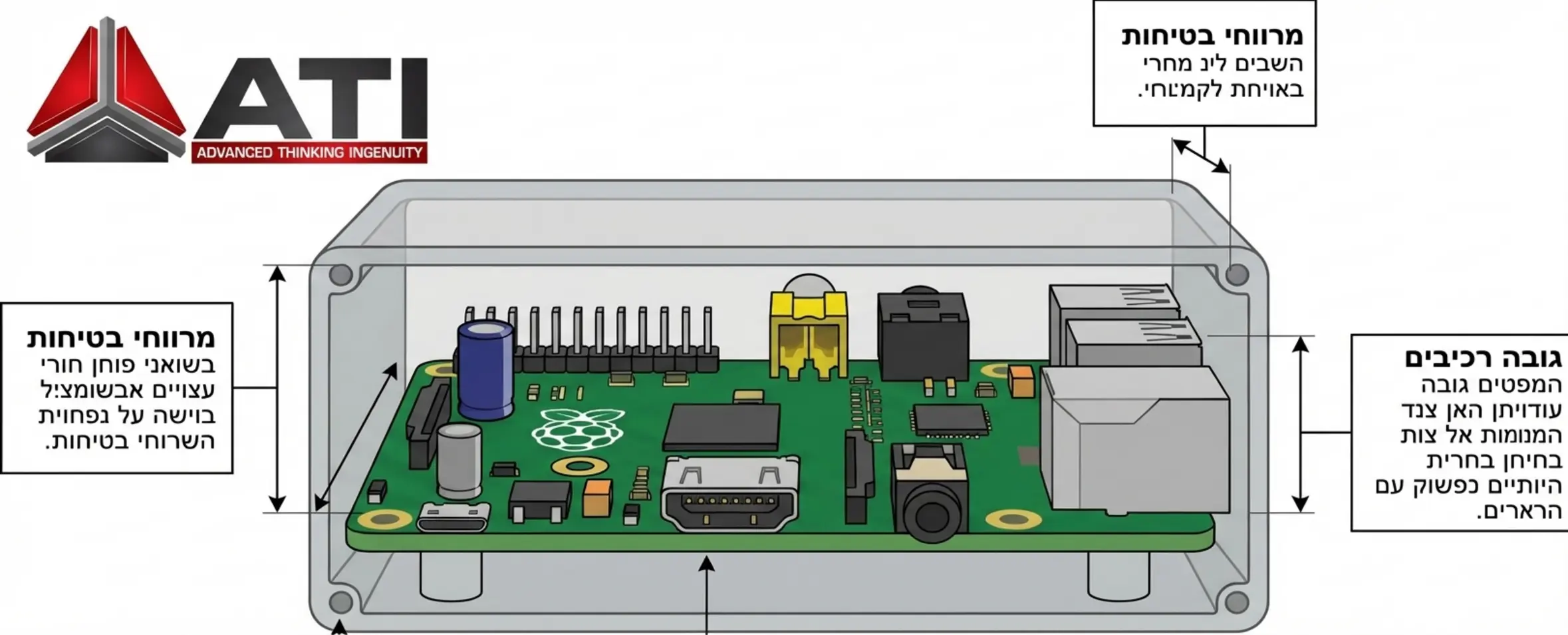
Another critical point is component height. Each area of the board has a height restriction derived from the internal structure of the enclosure. Tall components such as electrolytic capacitors, inductors, or heat sinks must be placed in areas where the enclosure cavity allows for it. Exclusion zones must be defined in the design system to ensure no component exceeds the permitted height.
Connector and End-User Access Placement
One of the biggest challenges in any product design process is integrating the external interfaces. Charging ports, communication connectors, buttons, and indicator LEDs must be accessible to the user in a convenient and logical manner. The position of connectors on the PCB must be synchronized to within a tenth of a millimeter with the openings in the enclosure.
A small deviation in board manufacturing or plastic injection can lead to a situation where a cable cannot be plugged into the socket. To address this challenge, tolerance stack-up analysis techniques are used. The mechanical engineer calculates the cumulative permitted deviations of all involved parts, ensuring that even in the worst case, the connector still fits its designated opening.
Additionally, connectors that endure constant mechanical stress - such as a charging port that is inserted and removed many times a day - must receive mechanical support from the enclosure. Relying solely on the solder joint between the connector and the board is insufficient, as it will eventually break. The enclosure should cradle the connector and absorb the applied force.
Management and Heat Dissipation Thermal
Heat is the greatest enemy of electronic components. As technology advances and components become smaller and faster, they emit more heat relative to their surface area. Poor thermal design will cause the product to overheat, degrade performance, and significantly shorten the device's lifespan.
When a circuit board is enclosed inside a housing, heat becomes trapped. The designer's task is to plan an efficient escape path for thermal energy. There are several key methods for addressing this challenge, and the choice depends on the product type, its power consumption, and the operating environment.
| Cooling Method | Description | Pros & Cons |
|---|---|---|
| Passive Cooling | Using ventilation openings in the enclosure for natural airflow, and using the enclosure body itself as a heat sink. | Very reliable, no moving parts, inexpensive. Limited effectiveness at high thermal loads. |
| Active Cooling | Integrating fans or small liquid pumps that force continuous flow of cooling media over the components. | Highly effective for dissipating large amounts of heat. Requires space and power, generates noise, and may fail. |
| Thermal Conduction | Using thermal pads that bridge between the hot component on the board and a metal part of the enclosure that dissipates heat outward. | Excellent for sealed enclosures (IP-rated). Requires a thermally conductive enclosure material, increasing manufacturing costs. |
Between EDA and MCAD Software Synchronization
Today, every serious product development process relies on advanced software that enables smooth data transfer between the electronic and mechanical domains. The process works bidirectionally.
In the first phase, the mechanical engineer exports the physical boundaries of the board - including mounting hole positions and permitted height zones - and transfers them to the electronics engineer. The electronics engineer imports the file and begins placing components according to the constraints.
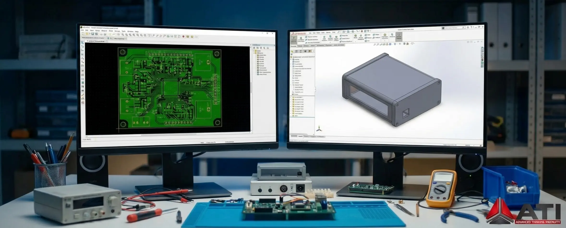
In the second phase, after the electronics engineer has placed the major components, a full 3D model of the board with all soldered components is exported. The mechanical engineer imports this model into the MCAD environment and runs an automatic collision check. If a specific capacitor penetrates the plastic wall, the software alerts immediately, and the placement can be corrected before the first board is manufactured.
Prototype and Physical Validation Testing
Despite the enormous progress in design software, there is no substitute for physical testing. The screen can tolerate anything, but reality may surprise you. That is why a mandatory step in every project is building an advanced prototype.
We manufacture the initial enclosure using high-quality 3D printing and simultaneously produce a first revision of the PCB. The first physical assembly is the moment of truth. There we verify whether the board slides smoothly into its dedicated rails, whether screws enter without forcing - which could warp the board - and whether connectors sit precisely in front of the openings.
Sometimes we discover that plastic manufacturing processes introduce small material shrinkages not accounted for in the computer model. The physical prototype allows us to make the final fine adjustments before transitioning to expensive mass production.
Standards, , and Regulation Compliance
Matching the PCB to its enclosure is not just a matter of dimensions and aesthetics - it is also about safety and compliance with international standards. Strict regulations dictate rules regarding the minimum required distance between high-voltage components and the external enclosure, especially when the enclosure is made of metal that could electrify the user. Familiarity with IPC standards is essential for every engineer working in this field.
If the device is intended for explosive, wet, or medical environments, clearance requirements become even more stringent. Development engineers must follow insulation standards and ensure that the mechanical design provides the required protection.
Common Design at the Board-Enclosure Interface Mistakes
Avoiding these pitfalls early in the design process can save significant time and cost:
- Ignoring enclosure coating thickness - Openings are designed to perfectly fit the connector, but paint or metallic coatings add thickness that shrinks the opening.
- Lack of center support for the board - Large boards tend to flex under the weight of components or when buttons are pressed. Support posts must be designed at the board center, not just at the edges.
- Forgetting internal cable routing - Many designs include cables connecting the main board to other elements like batteries or displays. Dedicated cable channels must be planned to prevent pinching when the enclosure is closed.
- Not considering disassembly for service - A product designed only for assembly, but which cannot be disassembled without breaking the board, represents a severe design failure that will prove expensive during technical support.
Steps to a Board-Enclosure Fit Perfect
Following a structured workflow ensures success:
- Define product requirements - Full characterization of the environment, standards, and user interface.
- Establish baseline dimensions - Mechanical engineer defines contour lines and initial restriction zones.
- Integrated design - Electronics engineer places components with continuous 3D model synchronization.
- Thermal analysis - Run heat simulations to verify cooling efficiency and plan dissipation paths.
- Collision check - Final digital verification of all system parts.
- Build prototype - Physical assembly, tolerance verification, and final corrections before production.

Tip From the Experts
Do not leave the mechanical design until the end of the electronics development process. The enclosure design and the PCB design must start together on day one of the project. Experience shows that this approach saves months of corrections and ensures a smooth, fast transition from prototype to mass production.
Key Takeaways
Parallel Design
Electronics and mechanics must be designed simultaneously from day one to avoid costly integration failures.
Thermal Management
Choose the right cooling strategy - passive, active, or conductive - based on power output and enclosure type.
Tolerance Analysis
Connector placement requires sub-millimeter accuracy with proper tolerance stack-up calculations.
EDA-MCAD Sync
Bidirectional 3D model exchange between electronic and mechanical design tools catches collisions early.
Frequently Asked Questions
At what stage of a project should I start matching the board to the enclosure?
The matching process must begin at the very earliest specification stages of the project. Immediately after formulating the concept and technical requirements, the mechanical and electronics teams must sit together to define the volume allocated for the board, connector positions, and the cooling strategy - before a single line is drawn in software.
How do you ensure board connectors align precisely with the openings in the plastic enclosure?
This is achieved by using 3D software that enables model sharing between the electronics and mechanical engineers. Additionally, a tolerance stack-up analysis must be performed that accounts for the natural imprecision of manufacturing processes, appropriate design clearances must be maintained, and the design should be validated with a 3D-printed prototype.
What happens when the PCB overheats inside a fully sealed enclosure?
In sealed enclosures, free air exchange is not possible for cooling. In such cases, trapped heat can destroy components. The accepted solution is using thermal pads that transfer heat from the hot components directly to the enclosure walls, which in turn act as a large heat sink dissipating heat to the external environment.
Does the enclosure material affect PCB design?
Absolutely. Metal enclosure materials, for example, provide excellent shielding against electromagnetic interference, but require larger safety clearances from any voltage-carrying component to prevent short circuits. Additionally, if the product includes an internal antenna, a metal enclosure may block transmission, requiring special plastic windows or an alternative plastic enclosure design.
What are the recommended safety clearances between the board edge and the enclosure wall?
As a rule of thumb, a clearance of approximately 0.5 to 1 millimeter should be maintained between the edge of the PCB and the plastic wall or guide rails. This clearance compensates for natural deviations in board cutting during manufacturing and prevents a situation where the board is forced in and suffers mechanical distortion.
How can a small change in an electronic component affect the entire enclosure?
Sometimes, due to global supply shortages, a component must be replaced with an equivalent that is a few millimeters taller. If that area of the enclosure was designed without safety margins, the new component may collide with the plastic cover. This situation requires either redesigning the board layout to relocate the component, or worse, modifying the injection mold for the enclosure - an extremely costly change.